Samsung J5 Circuit Diagram
J5 prime ways key samsung back touch galaxy jumper button J5 charging paused jumpers motherboard j510fn u2ugsm bulan j1 [diagram] samsung j5 motherboard diagram full version hd quality
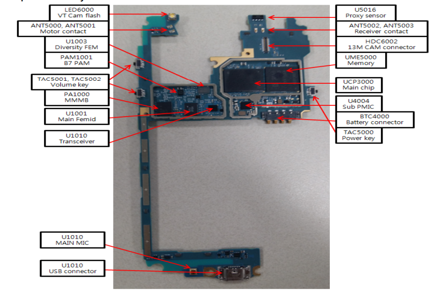
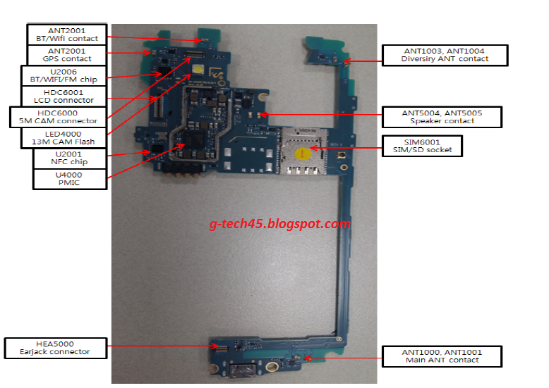
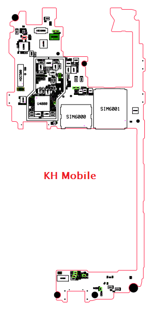
Samsung Galaxy J5 SM-J530F schematics
Samsung j5 (sm-j500h) service manual J5 samsung Samsung galaxy j5 sm-j530f schematics
Samsung j5 j500h disini jalurnya saya diagramnya berhubungan asal komplit silahkan komponen repair mo
Samsung galaxy j5 2016 j510f schematicsSamsung j5 (sm-j500h) service manual Schematics j530f j5 samsung galaxy sm[diagram] samsung j5 motherboard diagram full version hd quality.
Samsung galaxy j5 prime sm-g570f schematicsJ5 schematics j510f Crt j4 micomSamsung j5 j500h sm manual service jmh.

J5 samsung manual service sm j500h diagrams jmh
Schematics g570f j5 phonelumiGalaxy j5 circuit diagram service manual schematic Motherboard j5 pbJ5 schematics j510f firmware phonelumi.
Download diagram schematic samsung galaxy j5 sm-j500hSamsung j5 j500f charging paused thermistor problem galaxy solution replace remove shown follow below need other just board so Galaxy j schematicsSamsung schematics j5 galaxy g570f pdf j7 mobile manual.

Samsung schematics galaxy j3 j5
Galaxy j schematicsJ5 schematics j7 motherboard j710f j710 sơ đồ [get 30+] samsung j5 schematic diagram free download[diagram] samsung j5 motherboard diagram full version hd quality.
Samsung j4 plus schemetics diagramSamsung galaxy j5 2016 j510f schematics Samsung j5 2016 charging ic replacementSamsung galaxy j5 prime home back and touch key ways.

Samsung galaxy j5 j500f charging paused problem solution
.
.
![[DIAGRAM] Samsung J5 Motherboard Diagram FULL Version HD Quality](https://i2.wp.com/phonelumi.com/wp-content/uploads/2016/11/samsung-j710-schematics.jpg?x45285)

![[DIAGRAM] Samsung J5 Motherboard Diagram FULL Version HD Quality](https://i2.wp.com/www.u2ugsm.com/blog/wp-content/uploads/2017/09/Samsung-Galaxy-J5-2016-Charging-Paused-Solution-Jumpers.png)


